What Are the Challenges of BGA Assembly?
BGA assembly, challenging due to hidden joints and warpage, requires advanced techniques, skilled training, and strategic planning for reliable PCB production and minimized defects.
Among the most challenging processes in current PCB manufacturing and repair is BGA assembly. In BGAs, the components are directly attached to the circuit boards through solder balls on their bottom sides, which provide high-density interconnections needed for modern compact and high-performance electronics. Difficulty in BGA assembly involves dealing with preciseness in handling during placement, reflow, and rework processes. Special attention has to be taken while handling the challenges with the BGA assemblies to ensure reliable and successful assemblies. The following article discusses some of the common challenges related to BGA assemblies and strategic solutions for overcoming the same.
Introduction to BGA Assembly Challenges
The primary source of complication in BGA assembly emanates from the hidden nature of its solder joints. Unlike through-hole or surface-mounted components, BGAs mask their interconnectedness beneath the component itself. This prevents effective visual inspection of joint quality, and advanced techniques and equipment must be employed for high yield and functionality.
Common Challenges in BGA Assembly
Warped BGA
One of the most critical challenges arises as warping has become much more common with the BGA packages while they have been getting thinner and more fragile. The defects that may emanate from the warping include but are not limited to "Head in Pillow," where solder joints do not have any proper mechanical integrity. Such defects occur when the solder paste does not wet the solder ball fully owing to slight misalignment caused by warping of the package.
Solution: Warping can be minimized by optimization of the profile of reflow along with solder paste chemistry. The manufacturers can reduce the distortion effect by ensuring that there is a proper heat balance around the BGA. It is also ensured that there will be exactly correct bottom-side heating to provide maximum prevention from solder joint failure with maximum mechanical stability by using programmable multi-zone heating.
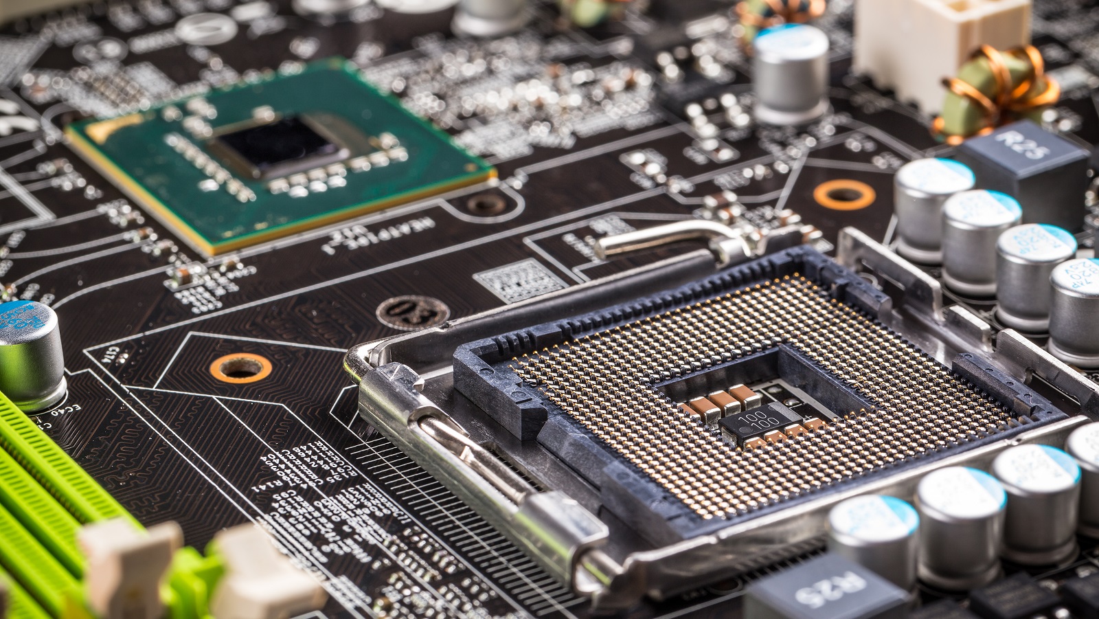
Neighboring Device Damage
As more and more components start to get placed on the board, simultaneously the danger of temperature-sensitive elements being around increases. It is common to know that devices such as ceramic capacitors, crystals, and connectors are susceptible to overheating during BGA rework and long-term reliability compromise.
Solution: Adequate thermal shielding is critical to protect these peripheral components. Traditional shielding methods, such as Kapton™ tape, have largely been replaced with new material technologies such as shielding clay gel or ceramic non-woven fiber. Relative to these older materials, these newer materials offer increased protection by minimizing thermal exposure and more convenience at assembly due to the elimination of requirements for cleaning the following application.
Underfill Rework
While underfill materials support mechanical stability and thermal management, they also pose a challenge during the rework process. As soon as the temperature of the reflow rises, the softening and expansion of these underfills make the removal process even more complicated. In addition, excessive mechanical force is applied with regard to the removal of the device, which further can cause damage either to the PCB or weakened solder pads.
Solution: High-speed milling systems are quite effective; they carefully grind off the cured underfill along with the residual solder balls without intense heat application. The precision in milling ensures less residual underfill is left, crucial to proper and reliable soldering at later stages of assembly. It reduces the impact of stress and vibration on the PCB, hence preserving it from structural and functional point of view.
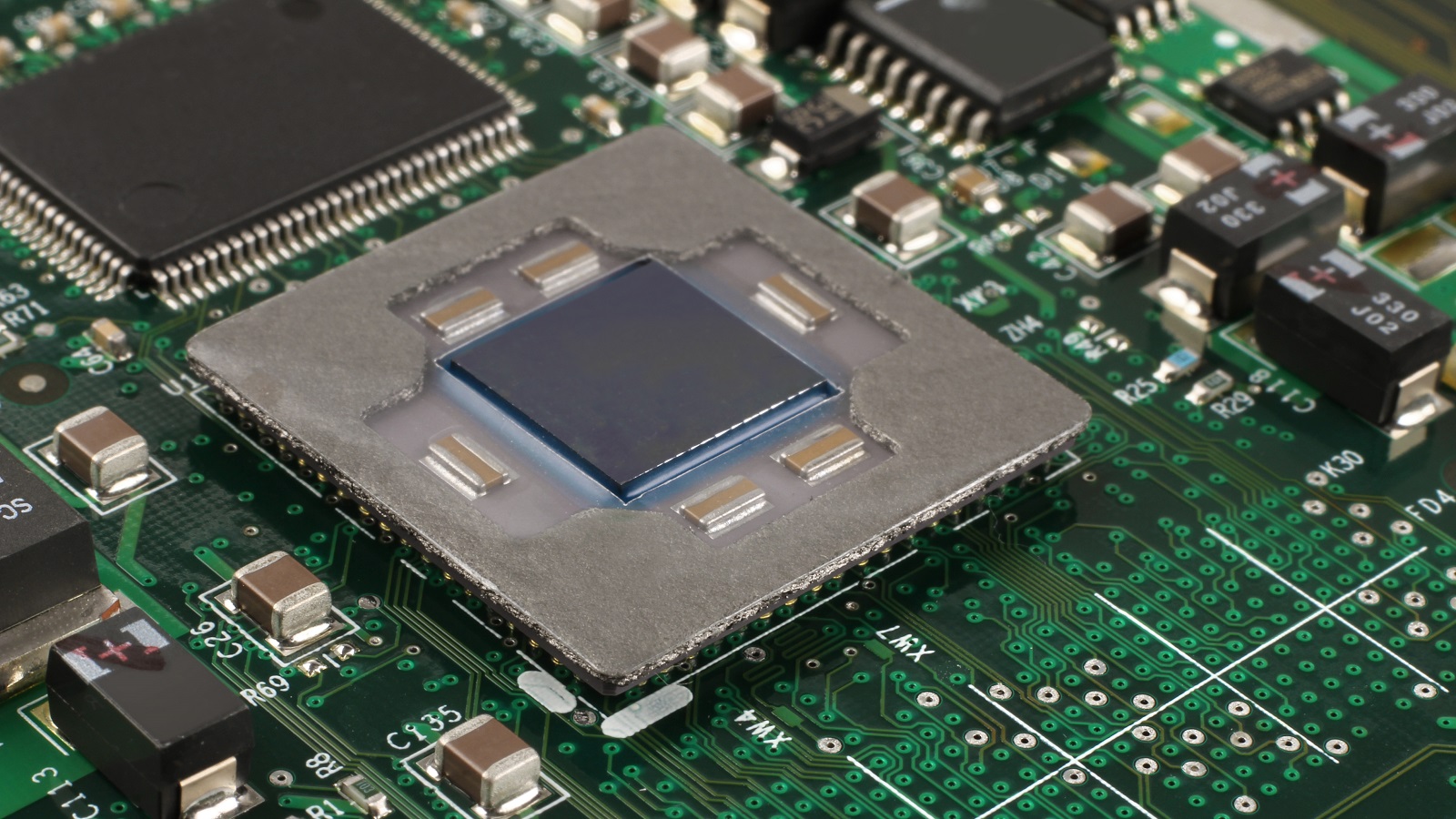
Overcoming the Challenges with Precision and Skill
Overcoming most of the problems with BGA assembly requires a combination of technology, technique, and talent. These include:
Investment in Advanced Equipment: Avail the latest rework stations and alignment tools that are capable of giving pin-point accuracy to BGA placement and rework. Such equipment enhances precision and reliability in assemblies.
Train and Develop Skills: Education and training of technicians are very necessary on a regular basis. Making technicians proficient to handle sophisticated tools and understand processes of rework will minimize the common occurrence of errors and hold quality intact.
Advanced Inspection Techniques: X-ray analysis and automated optical inspection-AOI. These methods are very important to get information about the integrity of solder joints, which otherwise would have remained hidden from the naked eye, thus allowing the possibility of their early detection and rectification.
Strategic Process Planning
Planning for the BGA assembly, right from the early design stages to the post-manufacturing stage, offers very minimal defects and the highest reliability:
Thermal Profile Optimization: Detailed thermal profiling for each variant of BGA so that warpage is less likely to occur and reflow conditions can be uniform.
Collaboration with Experts: In the same way, expert manufacturers and engineers will be contacted in both design and assembly processes for advice on how best to optimize the layout and select appropriate materials.
Proactive Quality Assurance: Have very high standards related to quality and institute mechanisms that ensure constant monitoring of the assembly process. This helps in maintaining a consistent high level of quality for the product.
Conclusion
Putting together BGAs requires a combination of precision, strategic planning, and skillful execution in order to rise above the challenges. It is within the purview of manufacturers to ensure robust and reliable BGA assemblies while continuing to guarantee premier standards of performance and quality in electronic products by embracing advanced technologies and refined processes. This does not only minimize incidences of rework and repair but also extends functional life for PCBs, thus enhancing their competitive advantage in dynamic technological environs.
Hot Tags:
Contact us

If you can't find what you're looking for, please contact us.
Article
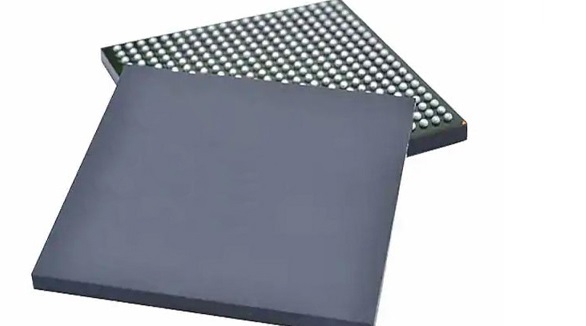
Compared to THT, SMT offers better miniaturization and weight reduction in any electronic application. With the use of BGA packages, high-assembly density, reliability, and improved performance are achieved; on the other hand, this requires a rework and inspection that is not really common. PCBX specializes in the area of advanced SMT and BGA assembly to help drive modern requirements of compact electronic devices.
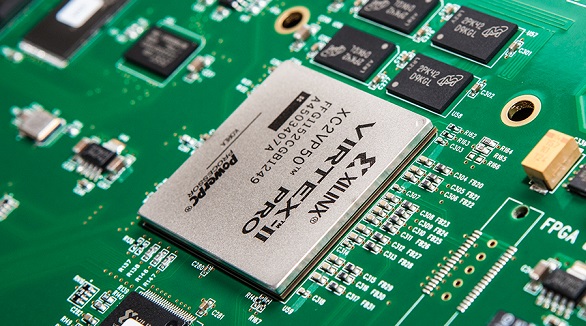
Ball Grid Array (BGA) components, such as PBGA, CBGA, CCGA, TBGA, and CSP, provide high I/O density, improved reliability, and high-quality electrical and thermal performance. Quality assembly and functionality are assured since advanced soldering and inspection methods are required, like AXI and AOI. Proper storage and handling shall guarantee the performance of the devices.
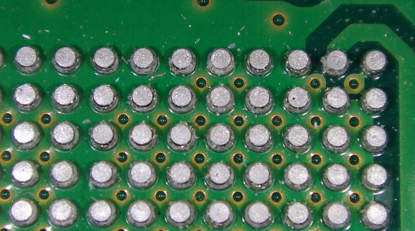
In the late 1980s, when electronics began to shrink, BGA packaging was developed to integrate more connections within a given area. Today, BGA is widely used with high-connection chips—processors being a good example. BGA uses solder balls at the bottom of the chip to connect it to the circuit board. It provides high density along with good heat dissipation and fast signal transmission, one of the main reasons it is ideal for modern electronics. However, it requires precise techniques of soldering in BGA manufacturing.